- English
- Español
- Português
- русский
- Français
- 日本語
- Deutsch
- tiếng Việt
- Italiano
- Nederlands
- ภาษาไทย
- Polski
- 한국어
- Svenska
- magyar
- Malay
- বাংলা ভাষার
- Dansk
- Suomi
- हिन्दी
- Pilipino
- Türkçe
- Gaeilge
- العربية
- Indonesia
- Norsk
- تمل
- český
- ελληνικά
- український
- Javanese
- فارسی
- தமிழ்
- తెలుగు
- नेपाली
- Burmese
- български
- ລາວ
- Latine
- Қазақша
- Euskal
- Azərbaycan
- Slovenský jazyk
- Македонски
- Lietuvos
- Eesti Keel
- Română
- Slovenski
- मराठी
- Srpski језик

Teardown of Apple’s New 140W GaN Fast Charger
2026-04-29
Apple's new 140W fast charger comes with a brand-new model A3607. As a brand-new charging accessory designed by Apple for next-generation devices, the exposure of A3607 has sparked widespread industry attention to the charging solutions of Apple's upcoming devices.
With its appearance, size and parameters basically the same as the previous model, has its internal architecture been adjusted? Have core components been upgraded? With these questions, ChargerLAB conducted a detailed teardown of the new Apple 140W fast charger A3607 immediately, and will now reveal its true internal structure.
Appearance of Apple 140W Fast Charger
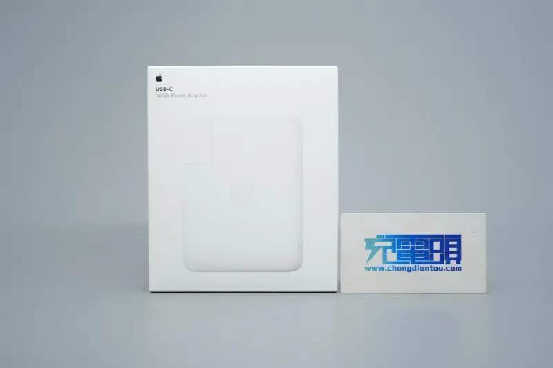
The packaging features a classic minimalist design, with the Apple logo, product name and appearance printed on the front.
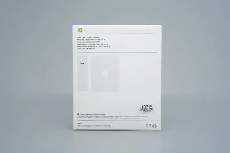
A product parameter sticker is attached to the side.
A close-up of the parameters on the sticker will be introduced in the product physical display section later.
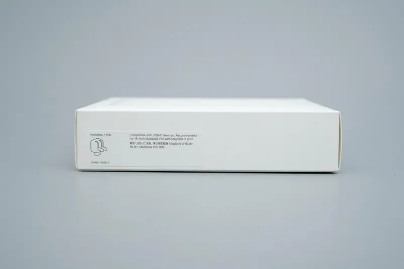
The charger is compatible with USB‑C devices, and is officially recommended for use with the 16‑inch MacBook Pro equipped with a MagSafe 3 port.
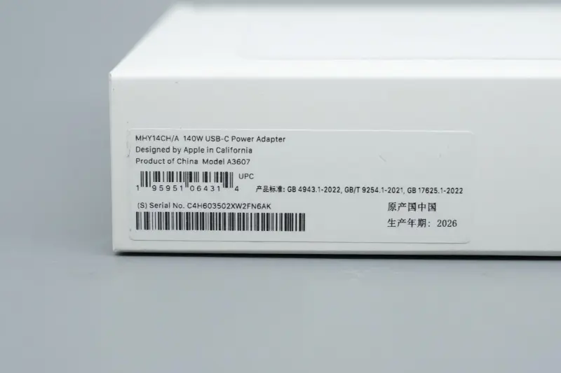
The power adapter is manufactured domestically, with a production date of 2026 and model A3607.
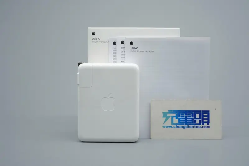
The package includes the charger and a user manual.
The charger is wrapped in a protective paper to prevent scratches in its initial state.
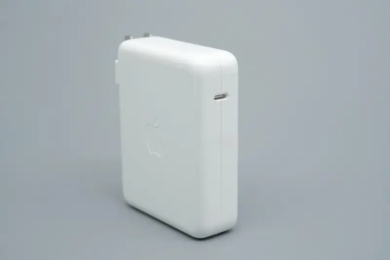
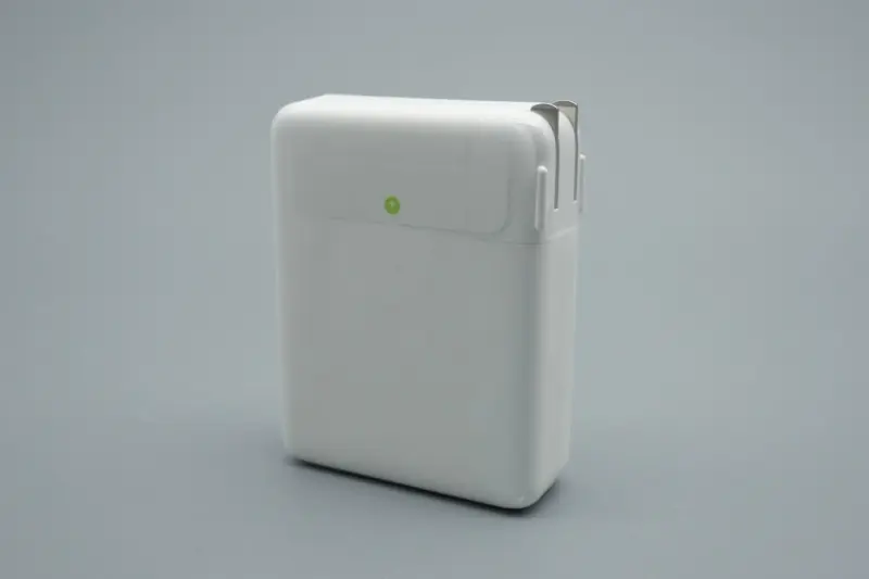
The appearance of Apple's new 140W fast charger is identical to the previous model, with a high-gloss glossy finish and rounded corner transitions.
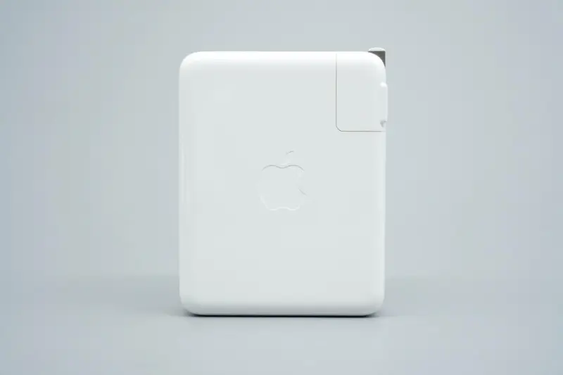
The Apple logo is centered on the front and back of the body.
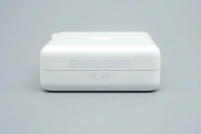
Parameter information of the charger is printed on one side of the body.
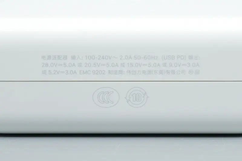
Product Parameters Close-up
Input: 100–240V~ 50/60Hz 2A
(USB PD) Output: 5.2V 3A, 9V 3A, 15V 5A, 20.5V 5A, 28V 5A
The charger has passed CCC and KC certifications.
The product name, model and precautions are printed on the other side of the casing.
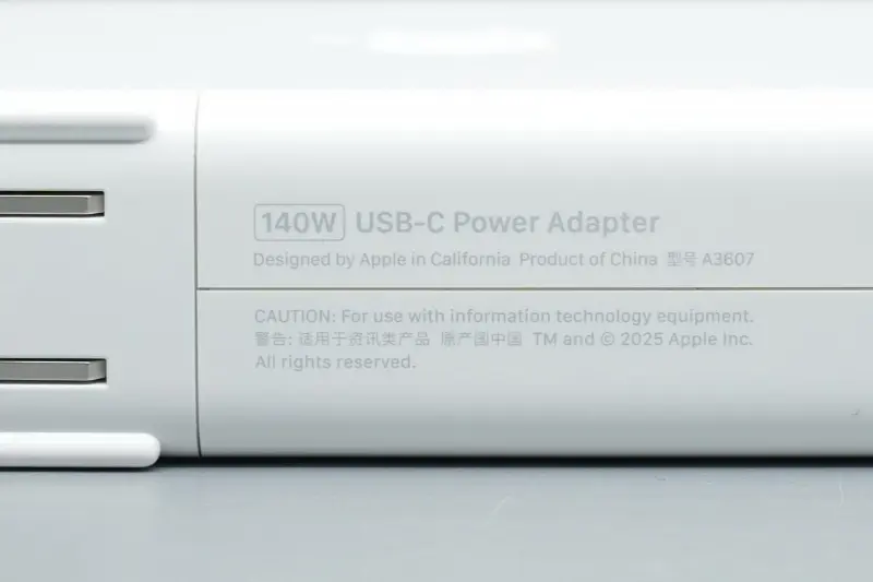
The model of Apple's new 140W fast charger is A3607.
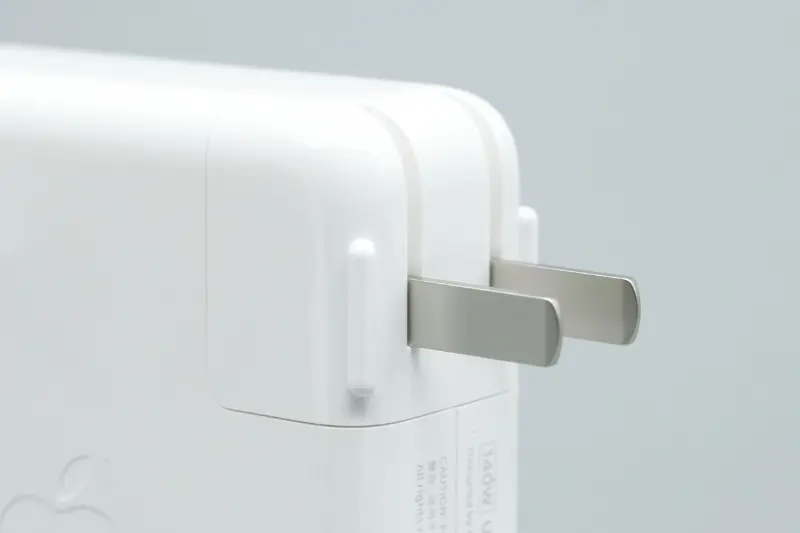
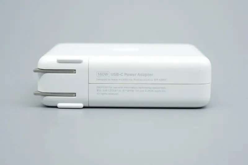
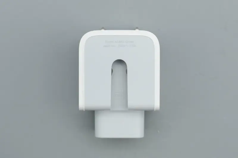
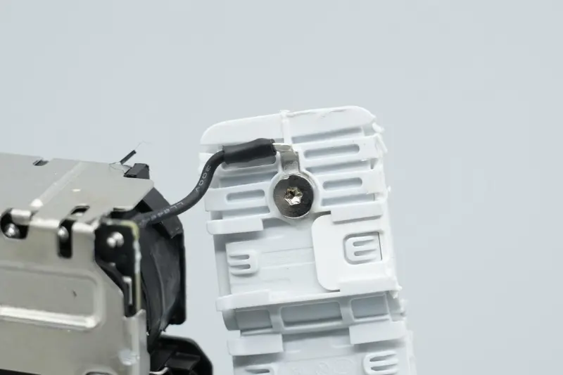
The charger is equipped with foldable standard Chinese pins, with dual-wing designs on both sides.
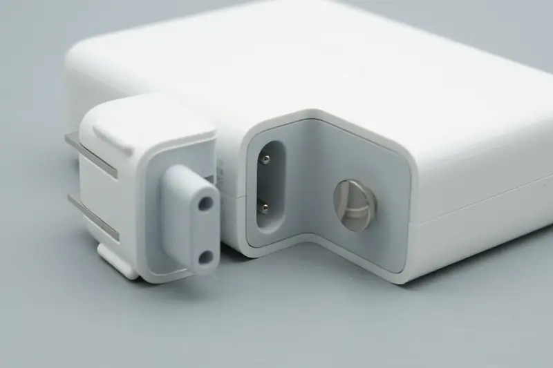
The pins adopt a classic independent module design and are detachable and replaceable.
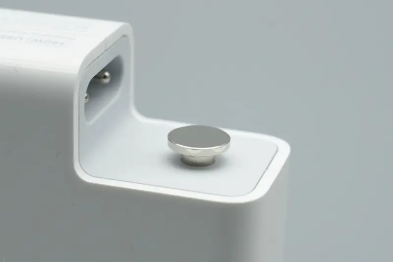
Close-up of the T-shaped fixing base, which can also serve as a grounding wire.
The module casing is marked with a rating of 250V~ 2.5A and Jabil Inc., indicating the pin module is supplied by Jabil. Notably, a metal clip for auxiliary fixation is added inside the module slot to ensure the module does not loosen easily after long-term use.
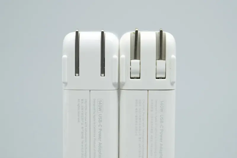
In addition, the pin design is different from the old version.
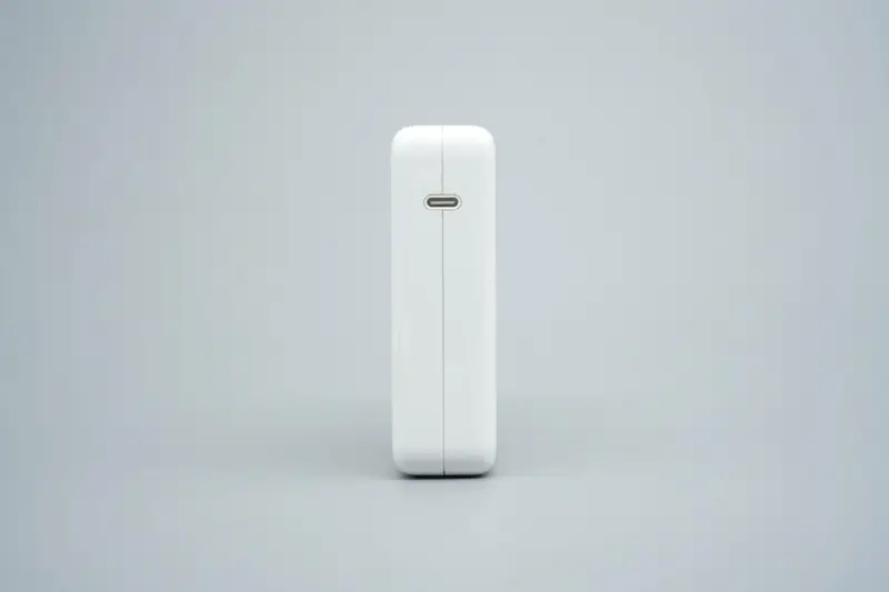
The output end is equipped with a single USB‑C port with a white plastic core.
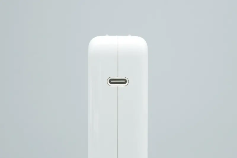
The USB‑C port receptacle shell is also independently designed.
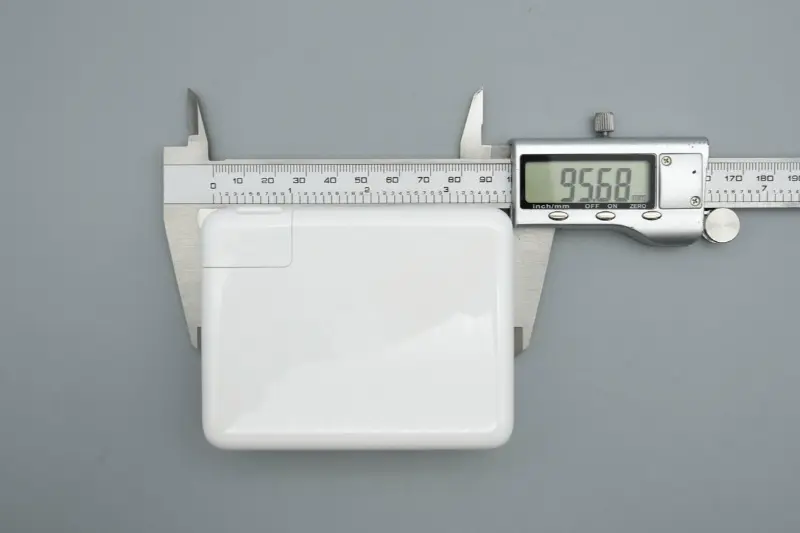
The measured body length of Apple's new 140W fast charger is 95.68mm.
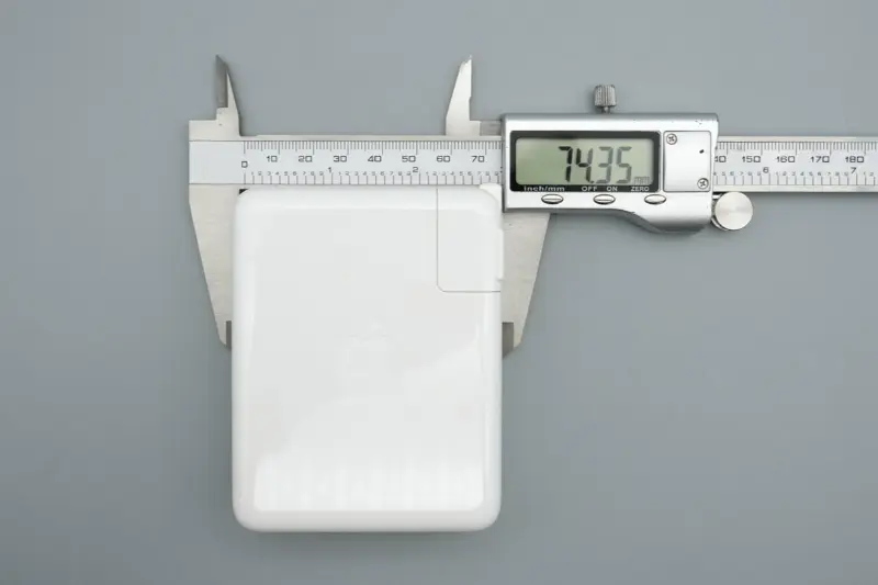
The width is 74.35mm.
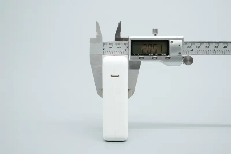
The thickness is 28.51mm.
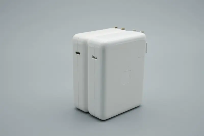
Placed side by side with Apple's old 140W gallium nitride fast charger A2452, the main appearance and dimensions of the new and old power adapters are completely identical.
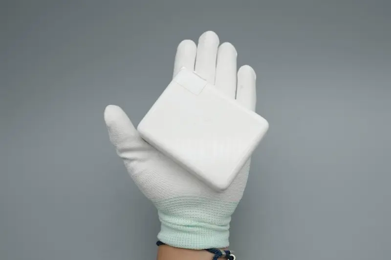
Intuitive size perception of the charger in hand.
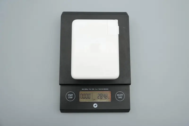
In addition, the product weighs approximately 285g.
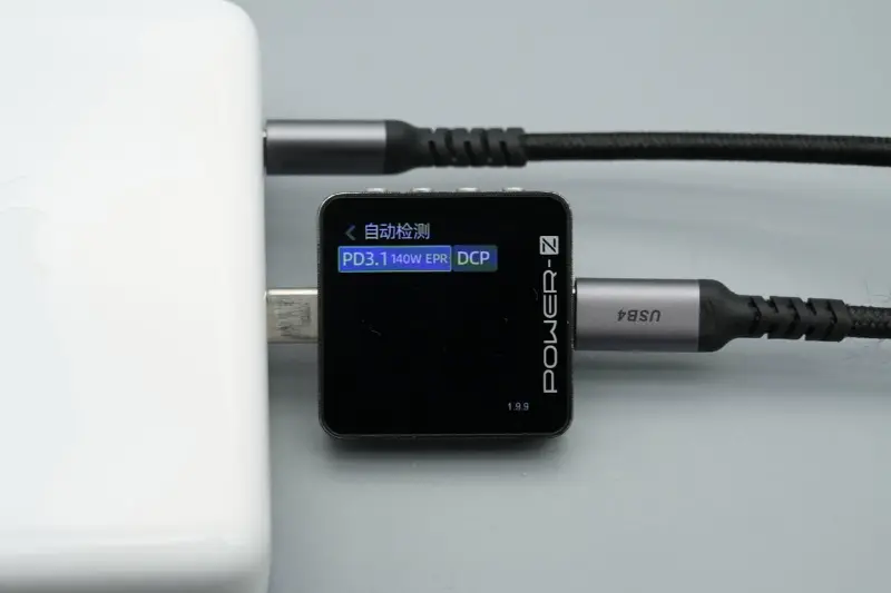
Tested with ChargerLAB POWER‑Z KM003C to detect the USB‑C port output protocol, it supports PD3.1 and DCP charging protocols.
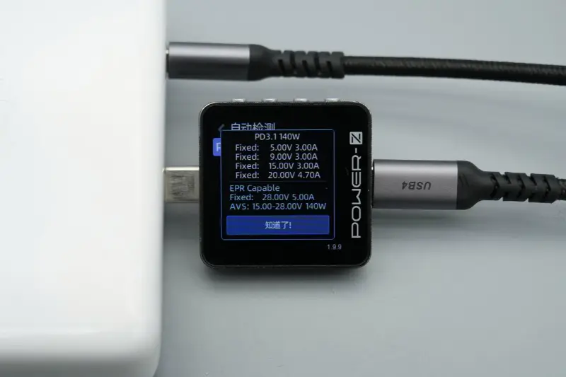
The PDO packet shows that the USB‑C port also has five fixed voltage gears: 5V 3A, 9V 3A, 15V 3A, 20V 4.7A, 28V 5A, as well as a 15–28V 140W AVS voltage gear.
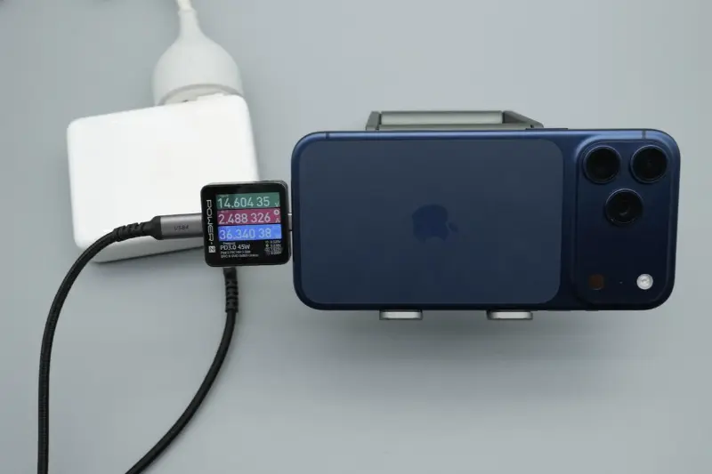
When charging an iPhone 17 Pro Max with Apple's new 140W fast charger, the measured charging power is approximately 36.34W.
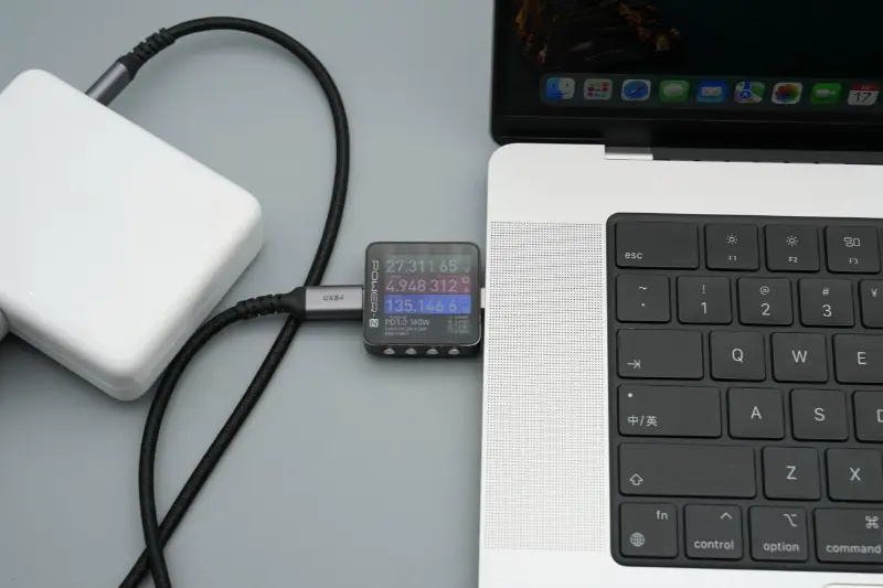
When charging a MacBook Pro, the measured charging power is approximately 135.15W, successfully enabling 28V 5A 140W fast charging.
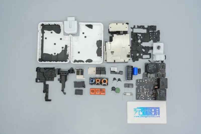
Teardown of Apple 140W Fast Charger
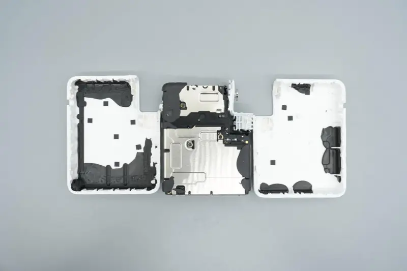
The charger casing is opened by cutting along the side.
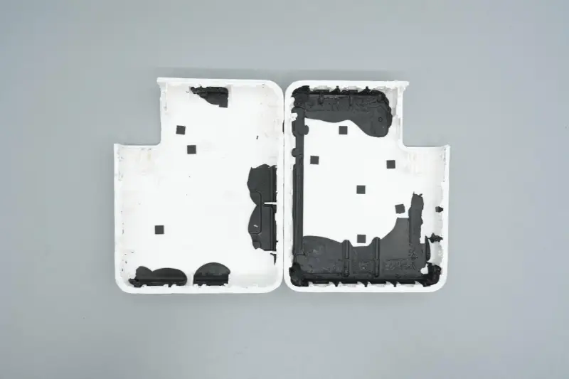
The casing is very thick for strong protection, and the edges are glued to reinforce internal modules.
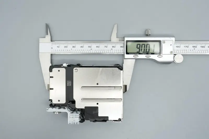
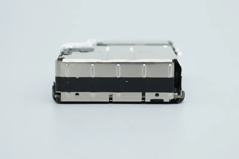
The measured length of the internal module is 90.01mm.
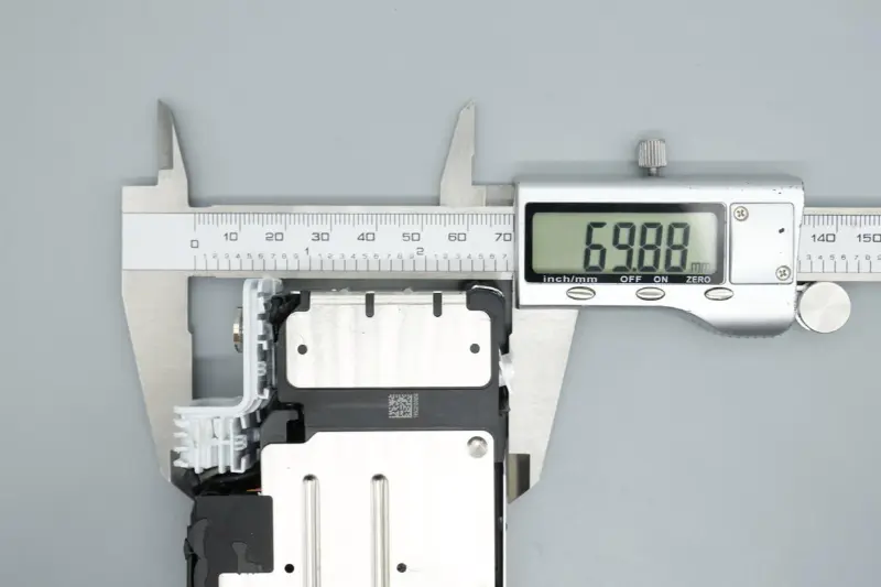
The width is 69.88mm.
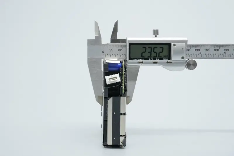
The thickness is 23.52mm.
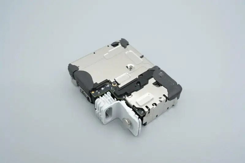
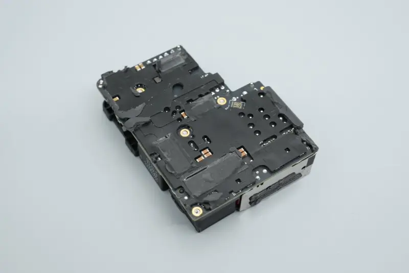
The PCBA module is covered with two integrated metal shells for uniform heat dissipation.
The metal shells are fixed with screws.
Insulation tape is attached to some areas on the side.
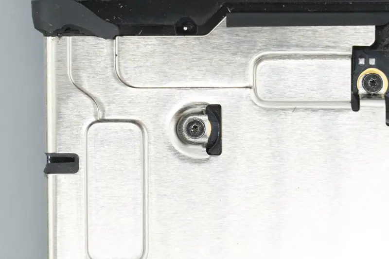
A wire at the input end is connected to the T-shaped fixing base for grounding.
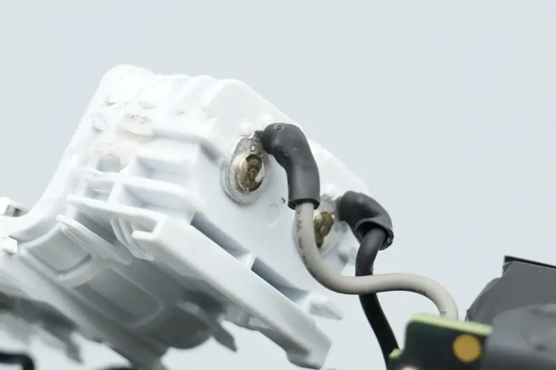
Heat-shrink tubing is used for insulation at the welding points of the AC wire terminals.
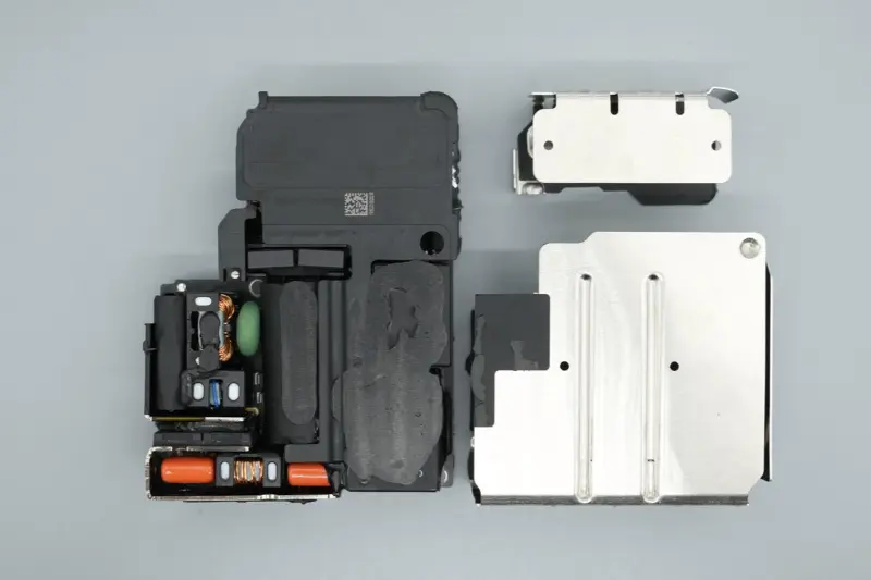
Remove the screws to take off the metal shells.
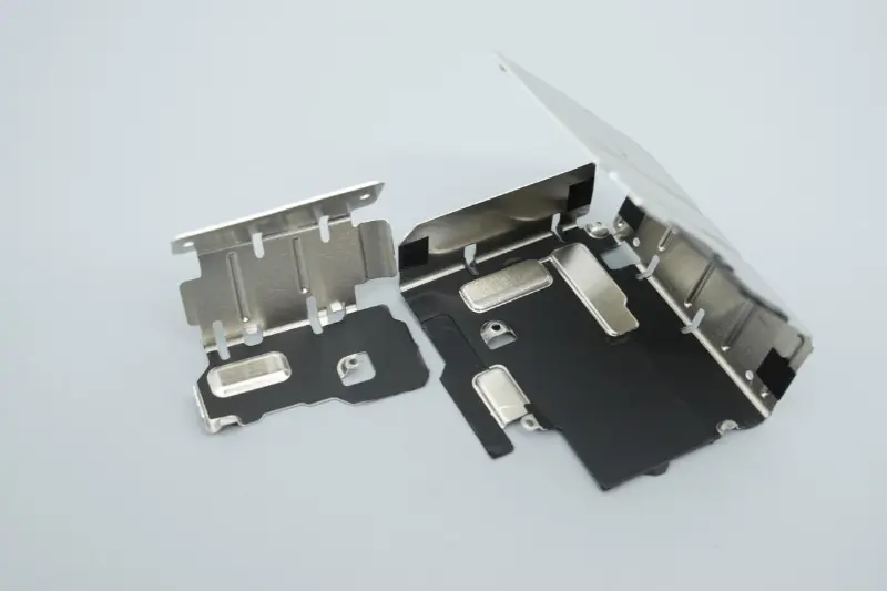
Insulation treatment is applied to the inner side of the metal shell corresponding to the back of the mainboard and other areas.
A plastic cover covers the transformer area of the module, and components such as capacitors and inductors are glued.
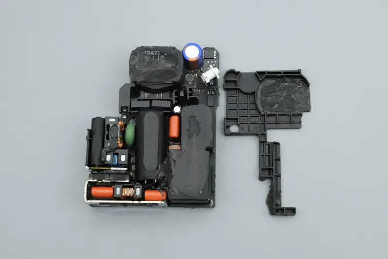
Remove the plastic cover, and a plastic frame is nested in the central area for reinforcement and isolation.
The back of the mainboard is covered with a soft rubber pad for protection.
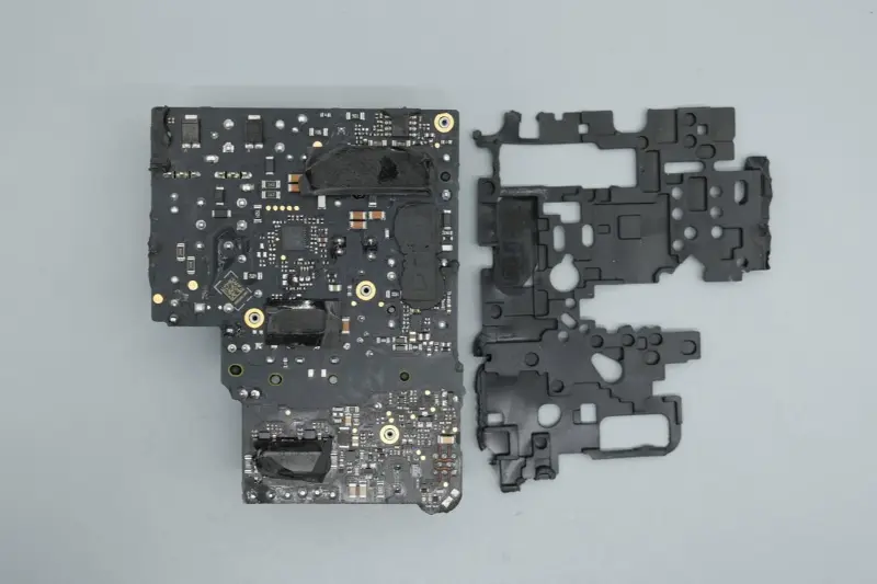
Remove the protective pad, and you can see that thermal conductive glue is applied to the corresponding chip areas and graphite thermal conductive stickers are attached.
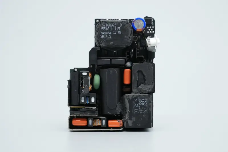
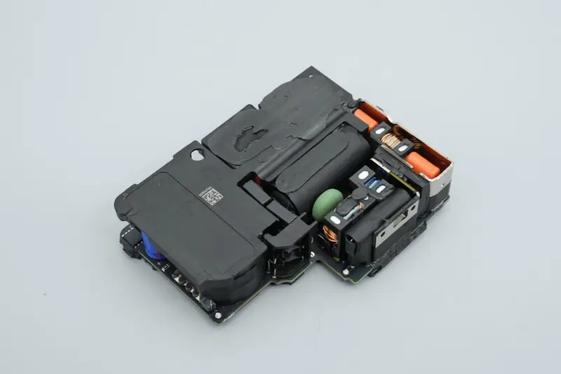
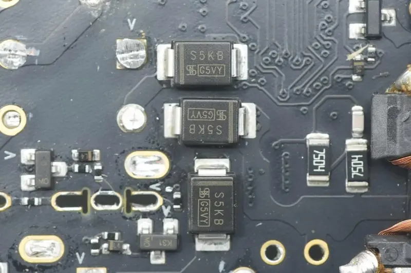
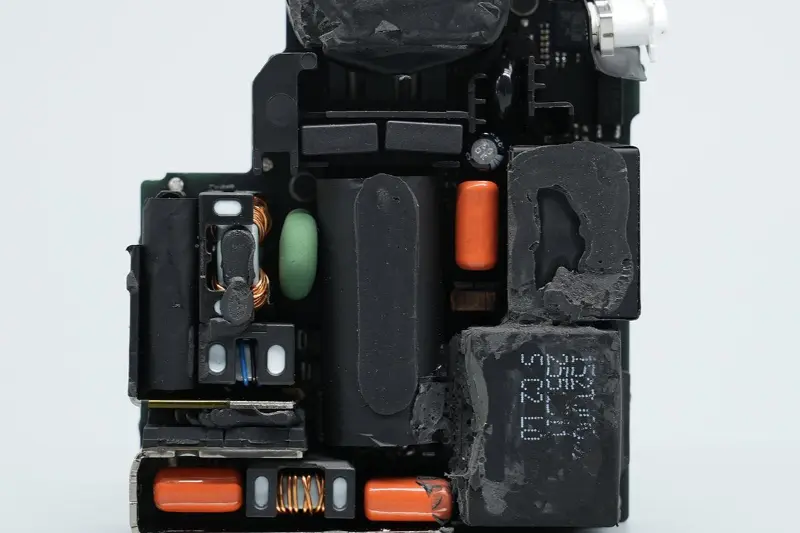
The front of the PCBA module is arranged with fuses, common-mode inductors, high-voltage filter electrolytic capacitors, current transformers, film capacitors, power supply capacitors, PFC boost inductors, step-down inductors, transformers and other devices, with a compact and orderly overall layout.
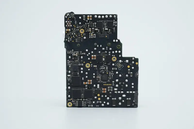
The back of the PCB board is equipped with relevant controllers and MOS tubes for the PFC boost circuit and LLC switching power supply circuit.
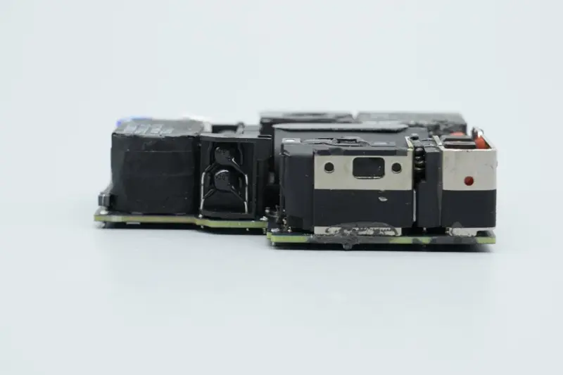
Two additional heat sinks are installed at the input end of the PCBA module, with two Infineon active rectifier MOS tubes in between.
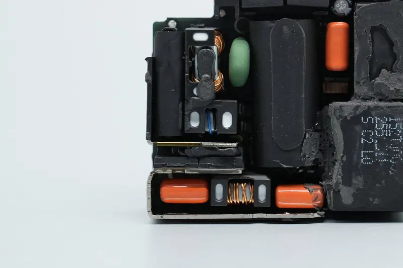
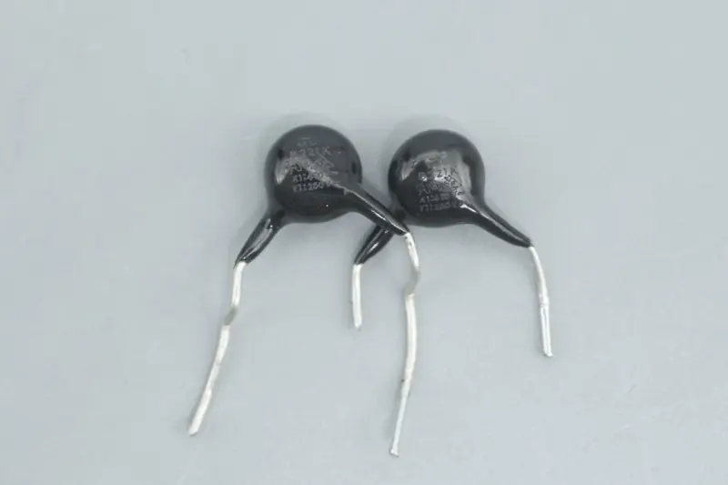
The area enclosed by the two heat sinks is also equipped with fuses, safety X2 capacitors, common-mode inductors, varistors, film filter capacitors, filter inductors and other devices.
The fuse is arranged on top of the safety X2 capacitor and wrapped with tape.
Peel off the tape, and you can see that the safety X2 capacitor is covered with a plastic shell for isolation, and the two components are wrapped and fixed with tape.
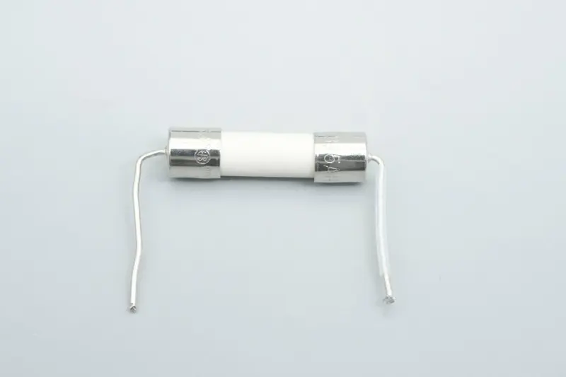
The rated current of the fuse is 3.15A, and an insulating tube is sleeved on one welding pin.
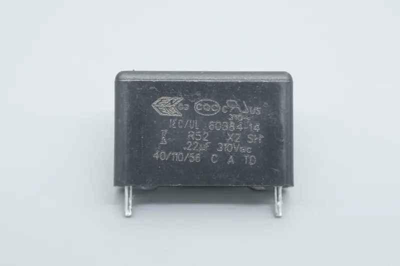
Close-up of the safety X2 capacitor with a capacity of 0.22μF.
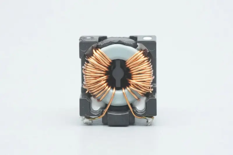
Common-mode inductors are used to filter out EMI interference, and are welded with plastic brackets.
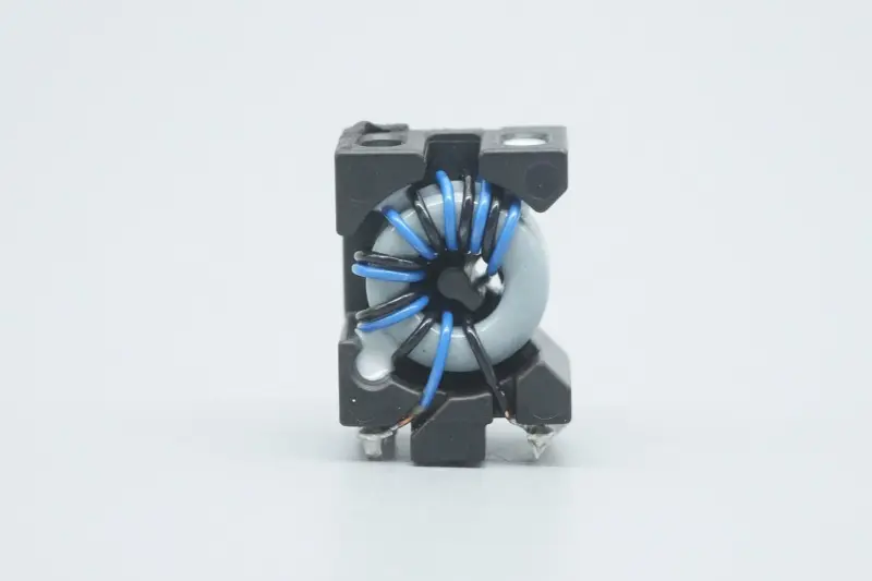
Close-up of another common-mode inductor.
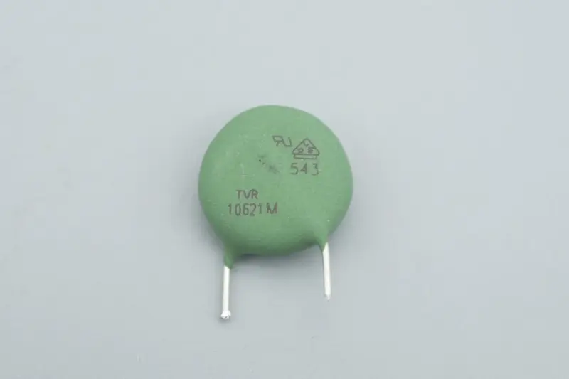
A TVR10621M varistor is used for input overvoltage protection.
The input end adopts a bridge rectifier composed of four diodes.
Close-up of the fourth diode.
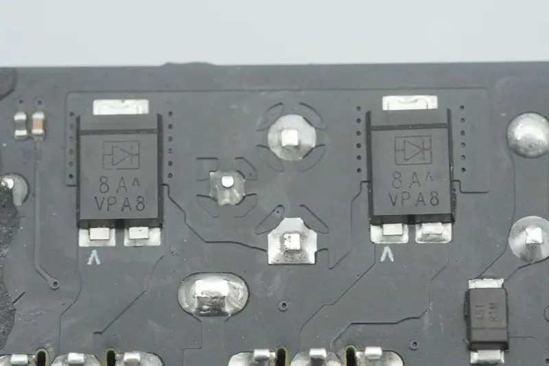
Close-up of the other two diodes, paired with Infineon CoolMOS IPA65R095C7 for active rectification.
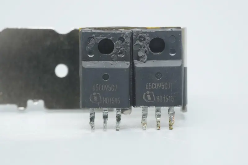
The two active rectifier MOS tubes are from Infineon, custom models for Apple, marked 65C095C7, packaged in TO‑220FP, used to improve rectification efficiency.
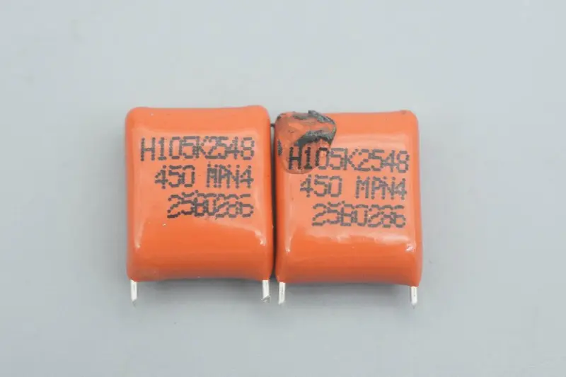
Close-up of two film capacitors with a specification of 1μF 450V.
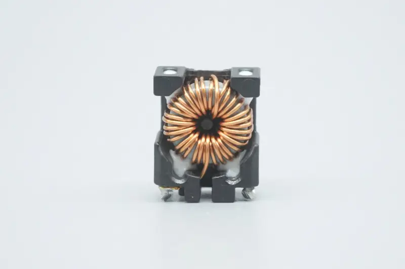
Close-up of the magnetic ring filter inductor, reinforced with glue.
A PFC boost inductor and a step-down inductor are installed at the other end.
The central area is equipped with high-voltage filter electrolytic capacitors, current transformers, film capacitors, resonant capacitors, main control chip power supply capacitors, Y capacitors and other devices. The high-voltage filter electrolytic capacitors are wrapped with insulating tape and placed horizontally.
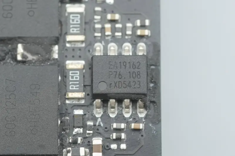
The PFC controller is from NXP, model TEA19162T, with integrated X-capacitor discharge function, operating in quasi-resonant mode or DCM mode. It supports an input voltage range of 70–276V, integrates soft start and soft stop, and provides precise boost regulated output.
TEA19162T adopts valley switching or zero-voltage switching to minimize switching losses, supports frequency limiting to reduce switching losses, and supports burst mode to reduce power consumption. Packaged in SO8.
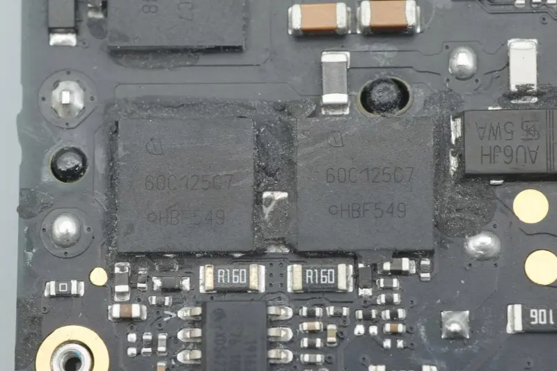
The PFC switch tube is from Infineon, marked 60C125C7, packaged in VSON‑4.
Close-up of the PFC boost inductor.
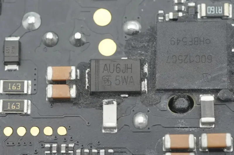
The PFC rectifier diode is from Taiwan Semiconductor, model TUAU6JH, a fast recovery diode with a specification of 600V 6A, packaged in TO‑277A.
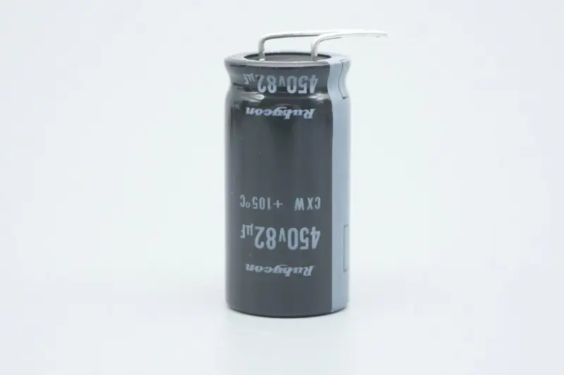
The high-voltage filter electrolytic capacitor is from Rubycon, with a specification of 450V 82μF.
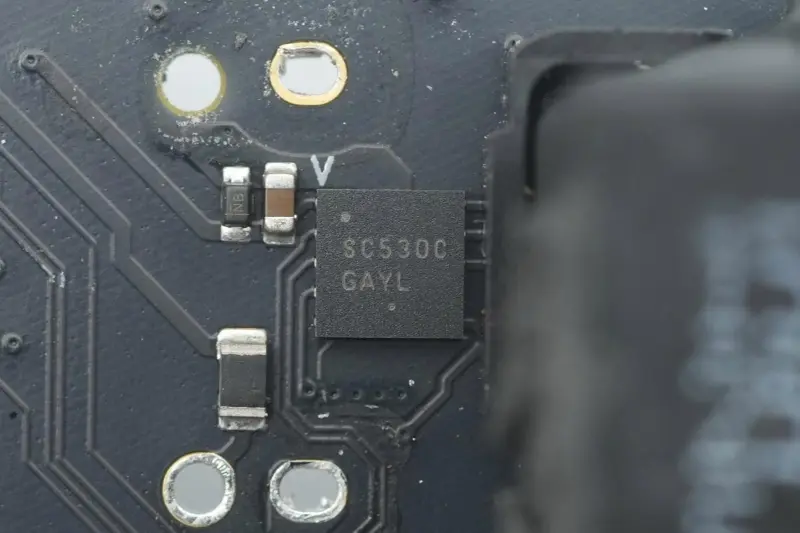
The driver for Infineon and STMicroelectronics switch tubes is a custom model from ON Semiconductor, marked SC530C.
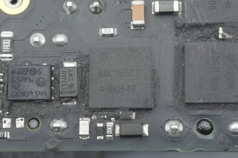
A custom MOS tube from Infineon, marked 60C185C7, a custom model for Apple, packaged in VSON‑4.
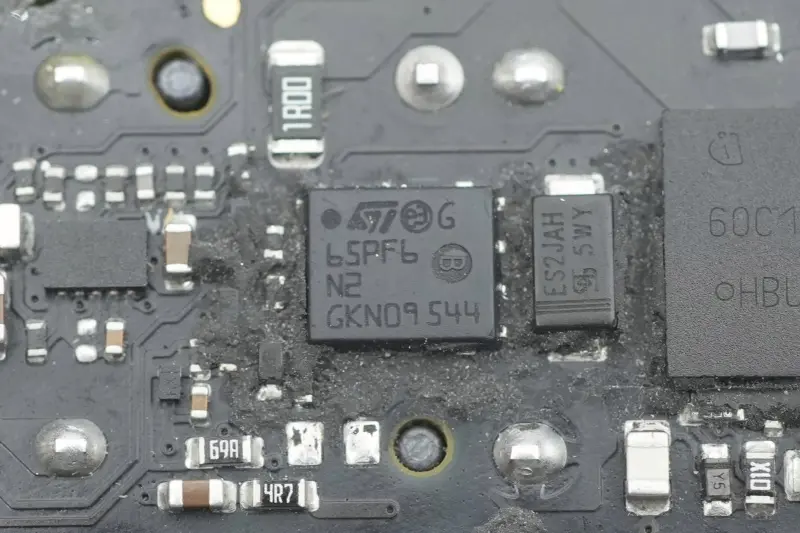
Another MOS tube is from STMicroelectronics, marked 65PF6N2, packaged in PowerFLAT 5x6 HV.
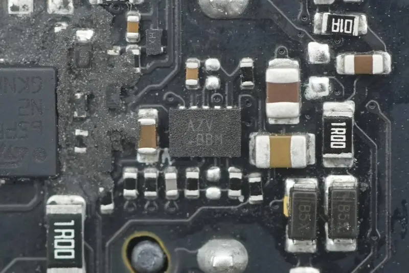
A chip marked AZV.
Current transformer for detecting the input current of the step-down stage.
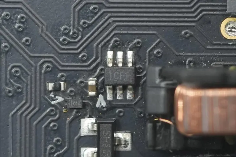
The dual-channel 1.65–5.5V inverter with Schmitt trigger input is from Texas Instruments, marked CFF, model SN74LVC2G14, packaged in SC70.
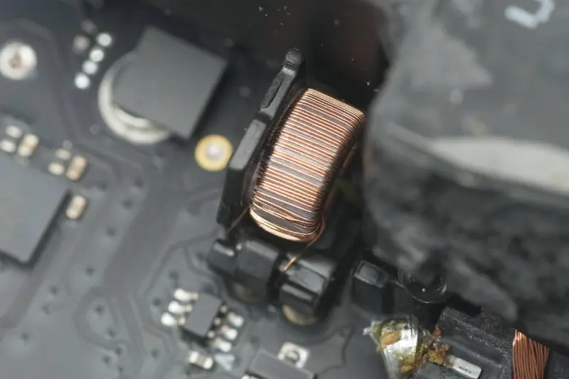
Close-up of the step-down inductor.
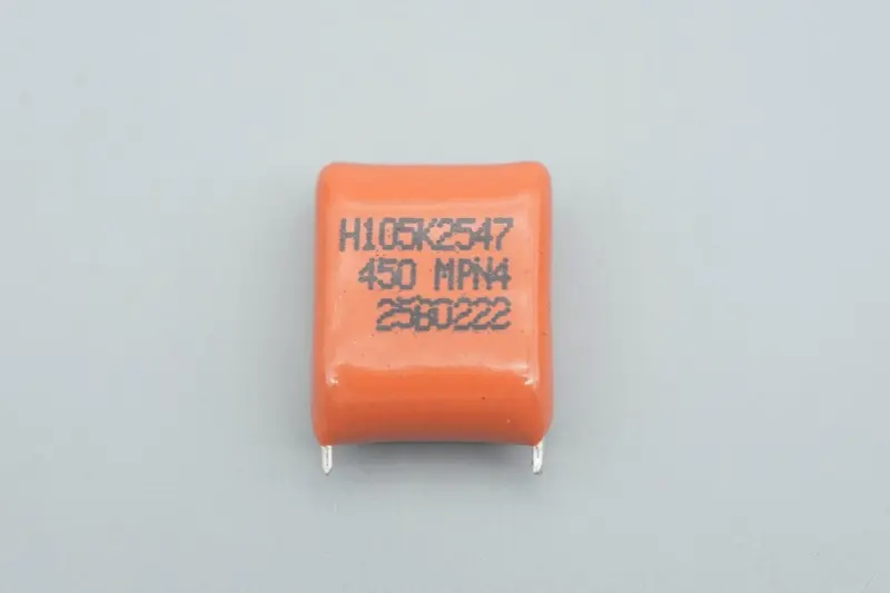
The third film filter capacitor has a specification of 1μF 450V.
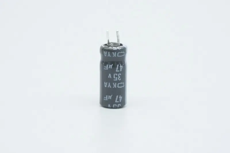
The main control chip power supply capacitor is also from Rubycon, with a specification of 35V 47μF.
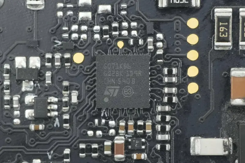
STMicroelectronics STM32G071KB M0 core MCU, built-in 128K Flash, 36K RAM, main frequency 64MHz, packaged in UFQFPN32, used for primary drive control of the power supply.
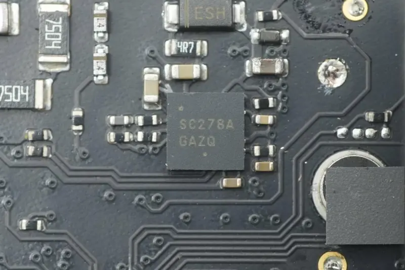
The driver for the two LLC switch tubes is a custom model from ON Semiconductor, marked SC278A, packaged in DFN‑10.
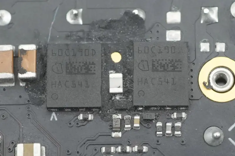
The two LLC switch tubes are from Infineon, marked 60C190D, custom models for Apple, packaged in TSON‑8‑6.
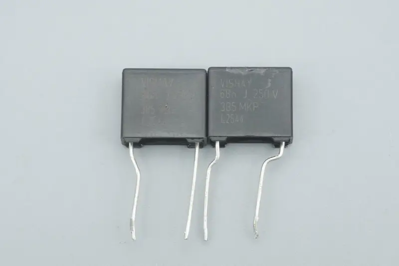
The two resonant capacitors are from VISHAY.
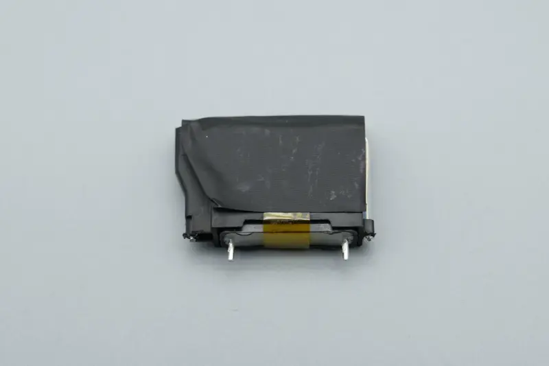
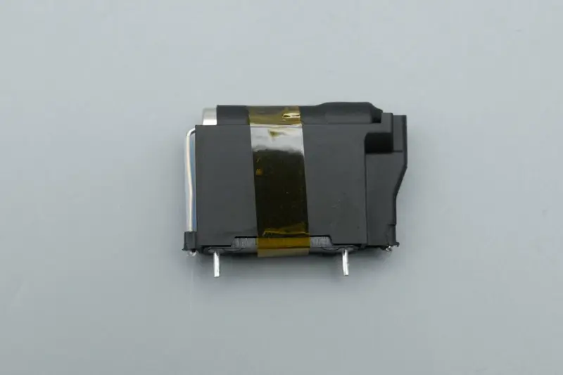
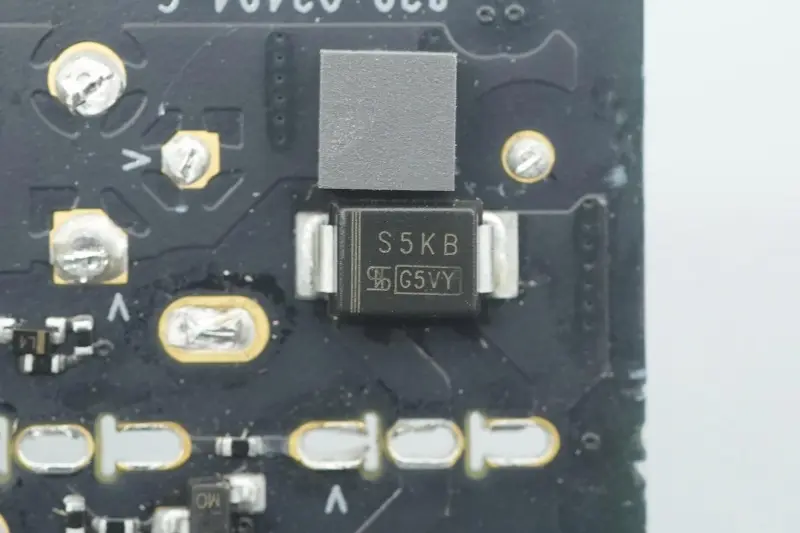
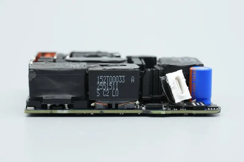
A transformer, optocoupler, output filter capacitor, protocol chip and VBUS switch tube are installed on one side of the output end.
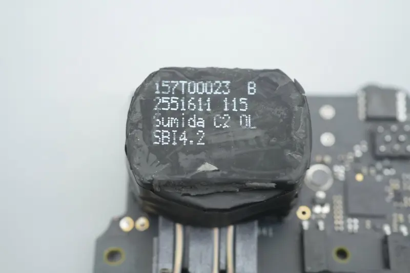
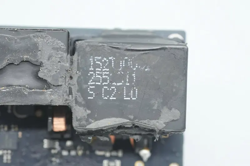
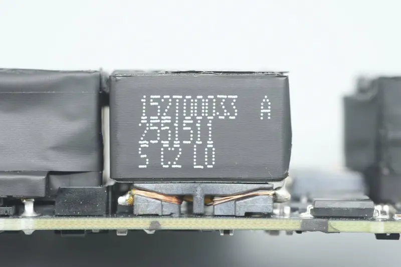
The transformer is supplied by Sumida.
Two black Y capacitors are used for anti-interference.
Close-up of two optocouplers, used for feedback output voltage and circuit protection.
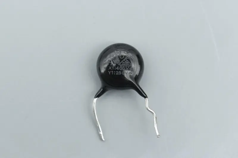
Close-up of the third Y capacitor.
Step-down converter for powering the synchronous rectification controller.
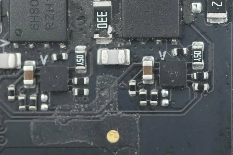
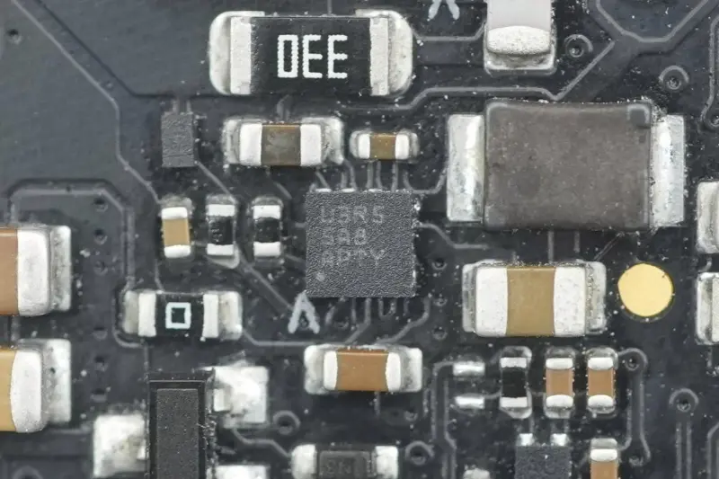
Two custom-model synchronous rectification controllers are from ON Semiconductor, marked TFV, packaged in WDFN8.
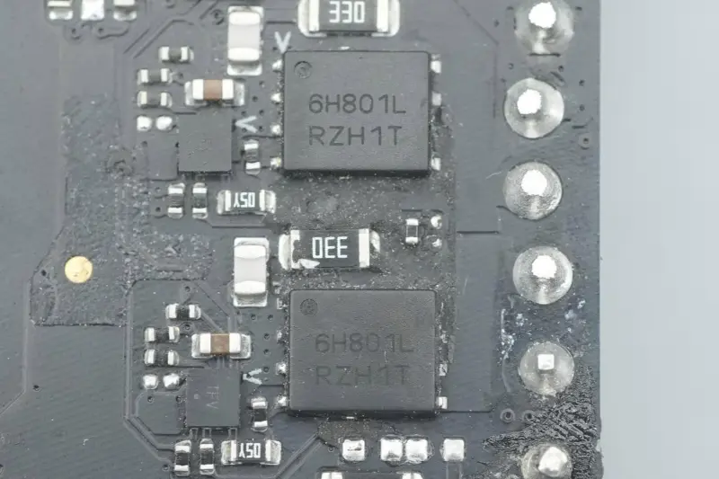
The synchronous rectifier tube is from ON Semiconductor, model NTMFS6H801NL, NMOS tube, withstand voltage 80V, on-resistance 2.7mΩ, packaged in DFN5.
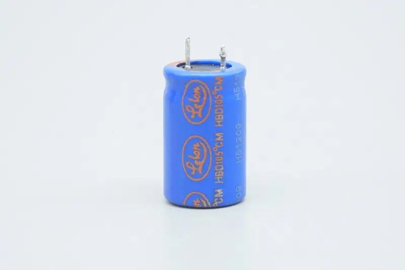
The output filter capacitor is from Lelon.
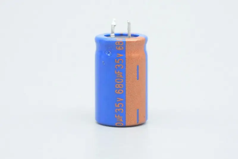
The capacitor specification is 35V 680μF.
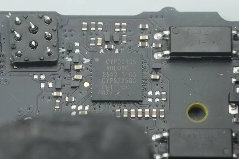
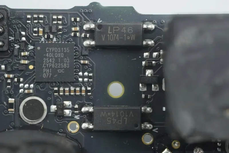
The protocol chip adopts Infineon CYPD3135, the industry’s first USB PD3.1 fast charging protocol chip, customized by Apple to Infineon.
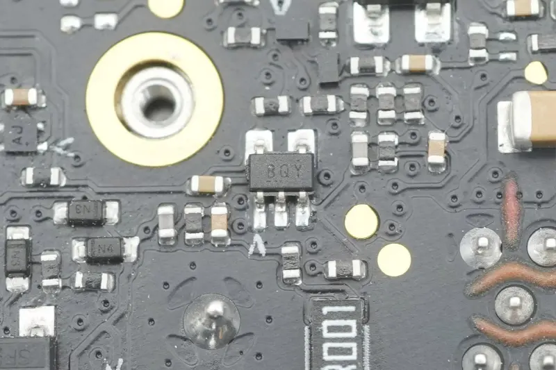
Amplifier for output current detection.
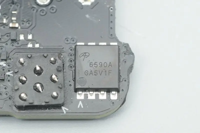
The output VBUS switch tube is from AOS, model AON6590A, NMOS tube, withstand voltage 40V, on-resistance 0.99mΩ, packaged in DFN5*6.
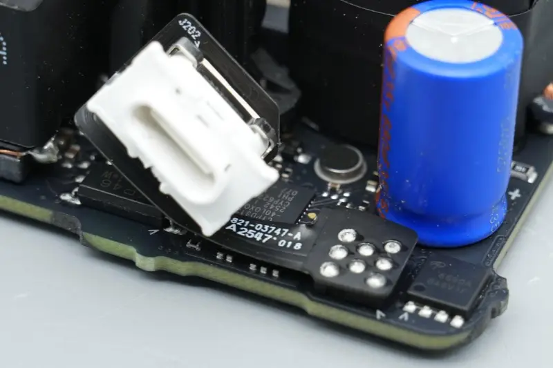
The USB‑C port receptacle is connected to the main PCB via a flexible circuit board.
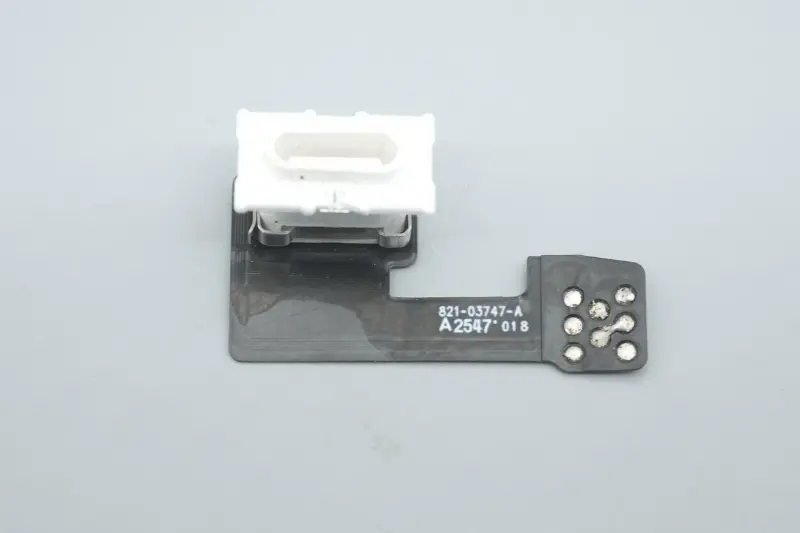
Close-up of the USB-C port receptacle.
Summary
Apple’s new 140W fast charger A3607 continues Apple’s consistent minimalist design language, and its overall appearance and size are highly consistent with the previous generation A2452. However, there are some detail differences: a metal clip for auxiliary fixation is added to the slot of the detachable pin module.
In terms of performance, while serving as the flagship power supply for Apple's new-generation devices, it is also highly compatible with previous old models, providing up to 140W PD3.1 fast charging for devices.
The charger still adopts a high-efficiency architecture of PFC + LLC + synchronous step-down, with a compact overall layout and solid heat dissipation design. In terms of core components, on the basis that the controllers are still chips of the same part number from NXP, STMicroelectronics, ON Semiconductor and Infineon, power devices are almost unified as Infineon's custom products, making the overall solution more intensive and customized, and energy efficiency performance is expected to be further improved.